Samsung Electronics Commercializes Gate-All-Around Processing to Scale Advanced High-Bandwidth Memory Yields
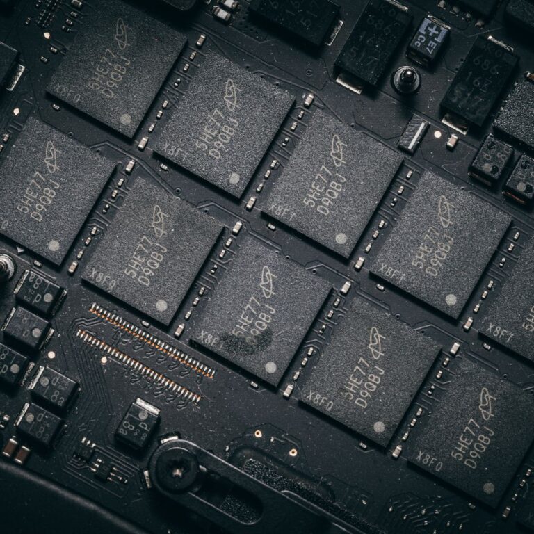
Samsung Electronics Commercializes Gate-All-Around Processing to Scale Advanced High-Bandwidth Memory Yields

삼성전자 has initiated full-scale optimization of its 2nm Gate-All-Around process to meet soaring production quotas for high-bandwidth memory and logic chips. This manufacturing shift addresses critical thermal and power bottlenecks in next-generation AI hardware accelerators.
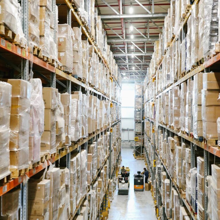

South Korean Policy Framework Directs Advanced Semiconductor and AI Infrastructure Expansion

Domestic semiconductor fabrication facilities are transitioning toward extreme ultraviolet lithography (EUV) process nodes to maintain competitive performance metrics. This equipment upgrade cycle requires specialized cleanroom environments and dedicated power supplies to handle high-density wafer processing without interruption.

Evaluating South Korean Advanced Semiconductor Manufacturing Initiatives for Global AI Infrastructure Growth

Domestic semiconductor manufacturing facilities are undergoing a major restructuring to support growing artificial intelligence hardware demands. Global market dynamics require high-volume fabrication lines to process denser circuit layouts without compromising wafer yields.

Strategic Scaling of Specialized Packaging Facilities in Korean Semiconductor Ecosystems

Strategic Scaling of Specialized Packaging Facilities in Korean Semiconductor Ecosystems

Strategic Scaling of Specialized Packaging Facilities in Korean Semiconductor Ecosystems The domestic semiconductor landscape is undergoing a structural shift toward advanced packaging technologies as a primary driver for high-performance computing demand. This transition requires a fundamental reconfiguration of how manufacturers …

Read more

South Korea Allocates Record Investment for Semiconductor R&D Infrastructure

The South Korean government has finalized an allocation of national resources for semiconductor research and development that represents an 역대 최대 (the largest ever in history) investment for the sector. This strategic funding aims to bolster the nation’s technological autonomy within the global supply chain, focusing specifically on next-generation computing architectures.

Korean Semiconductor Fabricators Expand Advanced Lithography Lines for AI Infrastructure

Korean Semiconductor Fabricators Expand Advanced Lithography Lines for AI Infrastructure

Domestic semiconductor manufacturers are expanding cleanroom capacity for extreme ultraviolet lithography (EUV) to support rising output demands. This physical expansion directly impacts production yields for high-density processors used in enterprise computing clusters.