Node Transition and Yield Benchmarks
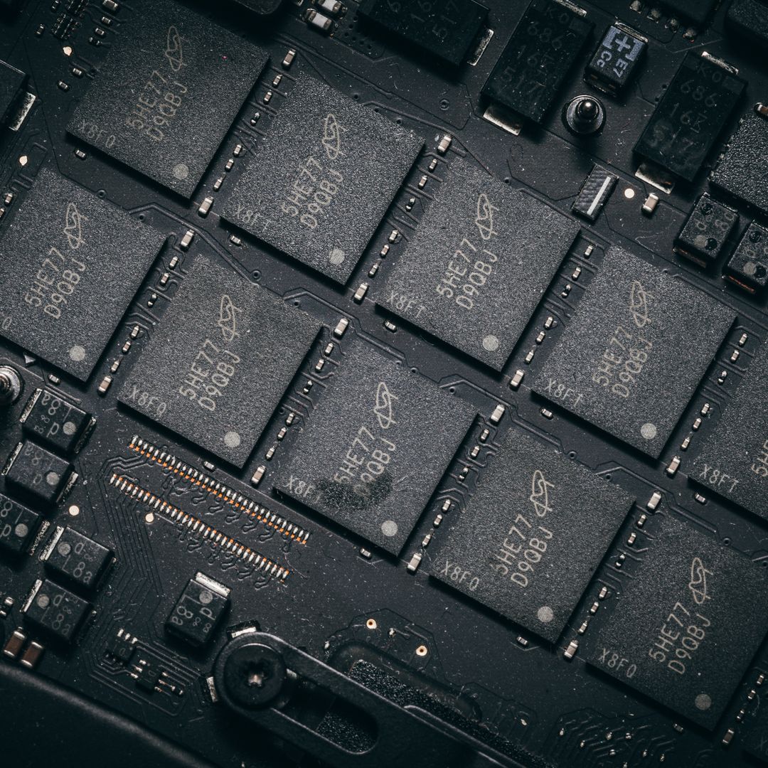
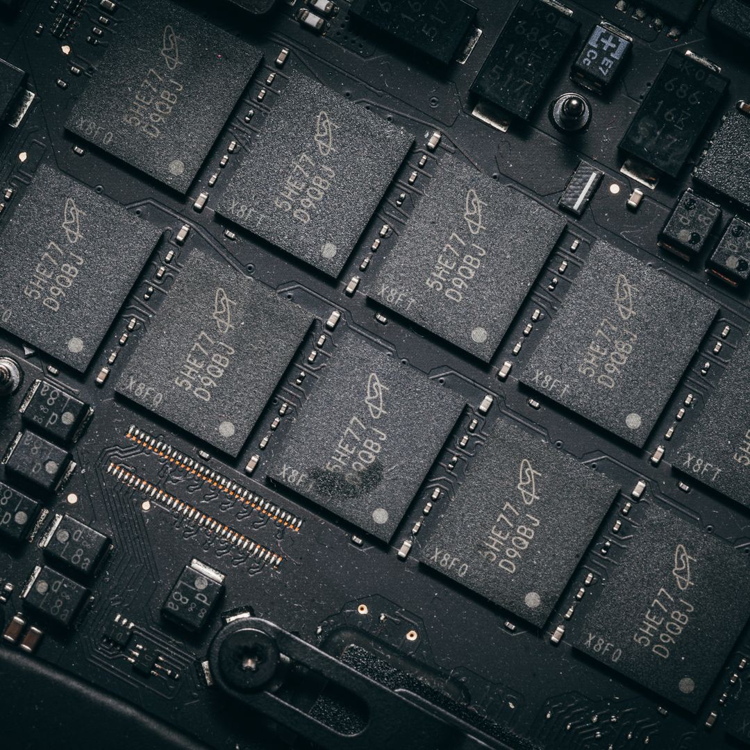
삼성전자 has initiated full-scale optimization of its 2nm Gate-All-Around process to meet soaring production quotas for high-bandwidth memory and logic chips. This manufacturing shift addresses critical thermal and power bottlenecks in next-generation AI hardware accelerators.
By shifting from conventional transistor structures, the semiconductor division aims to stabilize target wafer yields across key foundry lines in 2026. Global hardware vendors require stable silicon performance as deep learning workloads demand higher memory bandwidth and reduced energy leakage.
Technical Context: Gate-All-Around and MBCFET Architecture
The semiconductor industry relies on Gate-All-Around (a transistor architecture where the gate contacts the channel on all four sides) to overcome physical short-channel effect limits. Multi-Bridge-Channel Field-Effect Transistor (a proprietary variant using nanosheet channels to maximize current control) technology replaces older FinFET designs.
Controlling power consumption becomes essential when operational densities increase inside data center racks. The transition to nanosheet channels enables precise voltage tuning without inflating the physical footprint of the silicon die.
| Metric Parameter | FinFET Node Standard | 2nm GAA MBCFET Architecture |
|---|---|---|
| Gate Control Contact | 3-sided channel contact | 4-sided nanosheet surrounding contact |
| Operating Voltage Reduction | Baseline standard | Approximately 15% lower operational voltage |
| Drive Current Scaling | Constrained by fin height | Tunable via variable nanosheet width |
| Leakage Current Suppression | Moderate electro-static control | Superior sub-threshold channel isolation |
Institutional Research and Strategic Policy Alignment
National technological strategies actively support advanced logic packaging and next-generation memory fabrication across domestic semiconductor clusters. Policy frameworks directed by the Ministry of Science and ICT prioritize national hardware sovereignty and specialized chip design infrastructure.
Academic institutions provide essential fundamental research to resolve physical material limitations encountered at sub-2nm nodes. Advanced characterization studies conducted at KAIST focus on nanoscale defect reduction and inter-layer thermal dissipation within stacked logic architectures.
Evidence and Specifications for High-Bandwidth Memory Integration
Integrating memory and logic requires advanced hybrid bonding techniques to maintain signal integrity between stacked dies. Recent laboratory benchmarks confirm that micro-bump pitch reduction directly improves interconnect density between memory buffers and logic processing units.
Substantial capital allocation guarantees continuous production testing and process line calibration. Securing long-term institutional Investment enables continuous fabrication upgrades necessary for high-volume commercial runs in 2026.
- Interconnect Density: Hybrid bonding enables over 10,000 interconnects per square millimeter across stacked silicon structures.
- Thermal Dissipation Efficiency: Thin-film heat spreader integration reduces peak operational thermal hot-spots by up to 12%.
- Wafer Throughput Yields: Pilot line optimizations target steady yield thresholds suitable for commercial deployment by late 2026.
Industry Implications and Ecosystem Scaling
Foundry advancements extend beyond server compute engines to impact automotive silicon and power delivery systems. High-efficiency microcontroller units utilized in EV Battery management hardware benefit directly from sub-node leakage reductions.
Establishing open design kits lowers entry barriers for small-scale fabless chip developers trying to prototype custom accelerators. Local Startup ventures leverage shared multi-project wafer services to validate niche silicon intellectual property on advanced nodes.
Commercial Adoption Realities and Unknown Variables
Mass production scaling remains tied to economic cycle dynamics and global customer verification timelines. While pilot production lines demonstrate high stability, commercial yields under full volume production remain subject to rigorous client qualification tests.
Extreme ultraviolet lithography tool availability and raw substrate costs present ongoing operational uncertainties for domestic foundries. Long-term profitability will depend on maintaining high yield rates across diverse customer product layouts in 2026.
Primary Sources and Academic References
- KAIST: Advanced Semiconductor and Nanosheet Engineering Research Publications (https://www.kaist.ac.kr/en)
- Ministry of Science and ICT: National Strategic Technology Infrastructure Directives (https://www.msit.go.kr/eng)
자주 묻는 질문 (FAQ)
What primary technical innovation distinguishes Gate-All-Around from FinFET structures?
Gate-All-Around surrounds the channel on four sides using nanosheets, providing superior channel isolation and lower leakage current than three-sided FinFET designs.
How do institutional partnerships support Korean semiconductor manufacturing?
Research initiatives with KAIST and government frameworks from the Ministry of Science and ICT provide baseline nanoscale defect studies and technical infrastructure funding.
Get in Touch
Have questions about your specific situation? Reach out anytime for a personal consultation.