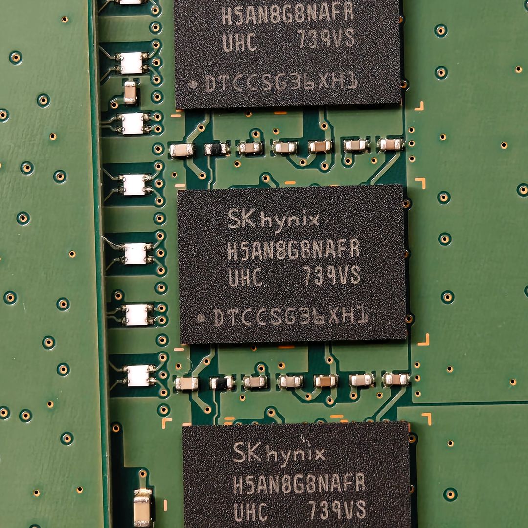

Current Production Shifts in Memory Architecture
Hynix is reorienting its manufacturing focus toward the high-density requirements of modern AI processing units. This transition involves scaling production of HBM (High Bandwidth Memory), which is critical for reducing latency in data-heavy operations.
Technical Requirements for Next-Generation Processing
Modern computational demands necessitate architectures that minimize the physical distance between memory and processors. The industry is moving toward vertical stacking techniques to improve bandwidth efficiency while managing power consumption constraints.
| Feature | Standard DRAM | HBM Architecture |
|---|---|---|
| Data Throughput | Moderate | Ultra-High |
| Physical Footprint | Large | Compact (Stacked) |
| Primary Application | General Computing | AI Training/Inference |
Institutional Collaboration and Research
Advancements in these architectures are supported by deep cooperation between domestic industry leaders and research institutions. The Ministry of Science and ICT (https://www.msit.go.kr/eng) provides the regulatory and funding framework necessary to maintain a competitive edge in global silicon manufacturing.
Parallel research at KAIST (https://www.kaist.ac.kr/en) focuses on developing new materials and logic-memory integration methods. These academic partnerships are essential for overcoming the physical limitations of current lithography processes.
Strategic Alignment with National Goals
Developing robust hardware is a central pillar of the national strategy to sustain long-term Tech News dominance. The integration of domestic semiconductor production into broader infrastructure projects ensures that local innovators have preferential access to high-performance components.
- Supply Chain Stability: Reducing reliance on foreign specialized components through domestic fabrication.
- R&D Synergy: Aligning private capital with public research objectives to accelerate prototype-to-production timelines.
- Cross-Sector Impact: Supporting the growth of peripheral industries, including EV Battery control systems and autonomous robotics.
Economic and Industrial Considerations
Market observers often track these capital expenditure cycles to assess the health of the broader technology sector. Detailed analysis of these trends is available for those monitoring long-term Investment performance within the domestic index.
The ability of the firm to maintain high yield rates on advanced nodes remains the primary metric for success in the coming cycles. Unexpected shifts in demand for specialized AI hardware could necessitate rapid adjustments to existing facility utilization rates.
Unresolved Technical Challenges
While current progress is steady, the industry faces persistent hurdles regarding thermal management in high-density chips. Engineering teams continue to refine cooling solutions that can operate effectively under the sustained workloads required by large-scale data centers.
The long-term viability of current stacking methods will be tested as manufacturers attempt to increase layer counts in 2026. Successfully scaling these processes remains the primary objective for the next phase of semiconductor development.
Primary Sources
- Ministry of Science and ICT, Policy Frameworks for Semiconductor Innovation.
- KAIST, Research Reports on Next-Generation Memory Architecture.
자주 묻는 질문 (FAQ)
What is the primary focus of Hynix in the current semiconductor market?
The company is prioritizing the mass production of high-bandwidth memory (HBM) to meet the intense data demands of modern AI processing architectures.
How do Korean universities contribute to semiconductor progress?
Institutions like KAIST conduct fundamental research on materials science and chip design, which helps manufacturers transition to more efficient, high-density production nodes.
Why is vertical stacking important for memory?
Vertical stacking reduces the physical distance between memory and logic circuits, significantly increasing data throughput and energy efficiency for AI-driven tasks.
What is the role of the Ministry of Science and ICT?
The Ministry provides the strategic policy framework and financial support necessary to secure the domestic semiconductor supply chain and foster innovation.
Get in Touch
Have questions about your specific situation? Reach out anytime for a personal consultation.